The Challenge
Traditionally, to bring down the cost basis of optical transceivers, the industry relied solely on economies of scale to drive supplier volume for all-optical subassembly supply chains. This stands in stark contrast to the multi-$100 billion silicon electronic supply chain which has benefited from shared design methodologies, automated wafer manufacturing, shared packaging approaches and common test infrastructure to deliver unparalleled economies of scale for computing and networking equipment. The optical transceiver industry, by comparison, is a cottage industry built on fractured design methodologies, captive wafer manufacturing, proprietary packaging and labor-intensive production that limits economies of scale.
In order to enjoy the same benefits as the silicon electronic supply chain, the optical transceiver industry needs a new approach to manufacturing that can scale, in both cost and performance, along with the rest of the networking industry.
Juniper’s Unique Approach to Silicon Photonics
For two decades, Juniper Networks has focused its engineering prowess to deliver industry-leading routing, switching and security solutions that, over time, adhere to a foundational principle: lowering the cost-per-bit in succeeding generations. Historically, this has been a key tenet in the development process for routing, switching and security, but the optics that interconnect them relied upon external market forces to lower the cost-per-bit. In recognition of this problem, Juniper acquired Aurrion, Inc. in 2016, a disruptive innovator in silicon photonics technology.
The intent of the Aurrion acquisition was to provide a path to materially impact the optical networking space as we know it. Silicon photonics is a ground-breaking technology that leverages the design methodologies and outsourced wafer manufacturing of the silicon electronic ecosystem to achieve economies-of-scale at the optical component level. The unique difference to Juniper’s approach is the integratration of all photonic elements of an optical transceiver—most importantly the lasers and the detectors—within a single silicon photonics die. This is achieved by integrating indium phosphide materials into a silicon process flow right on the silicon wafer—Juniper’s core intellectual property—to solve for a fundamental deficiency in existing silicon photonics technologies: the inability to amplify or generate light on chip.
The ability to incorporate all optical components within a single, common silicon die fundamentally changes and simplifies how an optical transceiver can be assembled and tested, dramatically reducing costs. The intellectual property that comprises Juniper’s silicon photonics platform differentiates it from any other silicon photonics platform in the market:
- At the die level, each of Juniper’s silicon photonics integrated circuits includes an optical loopback switch that allows the transmitter to be directly connected to the receiver. This enables the entire optical circuit to be tested during the manufacturing process using standard electronics-based wafer-level test equipment. Performing these tests before final assembly drastically improves the yield by identifying known good die without test escapes. The native optical loopback switch not only helps improve manufacturing yields, but can also be leveraged to perform in-service diagnostics while the pluggable optic is deployed in a live network, giving operators another tool to troubleshoot network issues remotely.
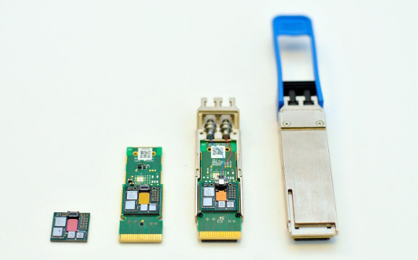
- At the “Opto-ASIC” transceiver package level, Juniper’s silicon photonics die is flip-chip-attached alongside other electronic ASICs to form a transceiver on a single, low-cost, ball grid array (BGA) substrate. This provides tremendous flexibility to how and where the transceivers are placed. By utilizing standard BGA package sizes, the transceiver package uses mature silicon testing methodologies making it easily adaptable to existing silicon manufacturing processes while maintaining stringent yield levels at high volume, further lowing the total cost to bring silicon photonics optics to market.
- At the module level, using a fully integrated silicon photonics platform transceiver permits a simplified printed circuit board design that only needs to accommodate the surface mounted transceiver package and DC-DC voltage converters. Fiber connection to the transceiver package is facilitated by a remateable connector that snaps into place with a clip. The resulting module architecture is easy to assemble and is yet another example of engineering simplicity with the silicon photonics platform for further cost reduction.

Figure 1: Juniper Networks’ silicon photonics enabled “Opto-ASIC,” a fully integrated transceiver package (left), surface mounted to module board (center left), board assembly placed within module housing with fiber attached (center right), and final QSFP module assembly (right).
Juniper’s silicon photonics technology leverages deep expertise in systems integration. This enables the silicon photonics platform packaging, in an optical pluggable transceiver module, to meet all standards-based specifications when used across any routing, switching or security platform. This additional level of compliance verification ensures that the transceiver modules are compliant and fully interoperable with any vendor’s networking equipment deployed today or in the future, allowing customers to deploy Juniper silicon photonics-based transceivers anywhere in their network while enjoying peace of mind of fully interoperable transceivers.
Future Applications of Silicon Photonics
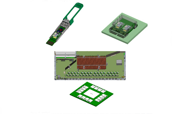
Juniper’s silicon photonics technology provides an entirely new approach to optics manufacturing that leverages design, wafer manufacturing, packaging and test infrastructure and methodologies from the electronics ecosystem, delivering the most advanced and cost-effective networking products. As new applications are introduced to the market, such as 5G, 8K video and AR/VR, the bandwidth requirements per individual router or switch will reach a point where networking vendors will be forced to re-engineer how these networking elements are architected. Juniper’s fully integrated “Opto-ASIC” transceiver provides a novel approach forward with its ability to densely package electronic and photonic die in a single, low-cost package, and it is completely agnostic to being packaged in existing module form factors (QSFP, QSFP-DD, OSFP, COBO, etc.). While packet processing capabilities of network processor chips keep increasing exponentially, the ability to push that much bandwidth in and out of the network processors electrically is hitting the brick wall of Shannon’s law. There is a clear inflection point approaching us where the only way to increase the throughput of the network processors is to directly integrate photonics on the same package as the network processor.
Juniper’s unique silicon photonics technology could also be incorporated into future Juniper packet forwarding engines, along with Penta Silicon and Triton Silicon, providing an entirely new generation of scaling performance at the linecard and system level, to enable petabit-per-sec total system capacity. By combining our silicon photonics technology and our network processors, the sky’s the limit for system level capacity, power consumption and performance.

Figure 2: 400GbE Opto-ASIC packaged in a QSF56-DD module (top left), 2x400GbE in COBO module (top right), 64x400GbE on-board-optic array (32 on front, 32 on back) integrated within a switch chassis (bottom left), and Opto-ASICs co-packaged with a packet forwarding engine to enable maximum bandwidth density (bottom right).


